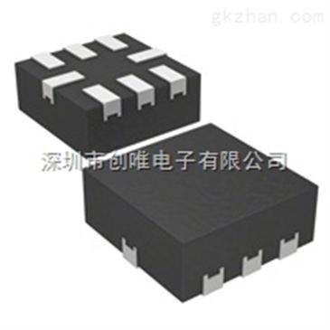
ADI公司的ADN4624是四通道信号隔离式低压差模信号(LVDS)缓冲器, 数据速率高达2.5 Gbps,并且具有极低的抖动.该器件集成了ADI公司的iCoupler®技术, 针对高速运行进行了增强,可提供LVDS信号链的插入式电气隔离. 到LVDS接收器和来自LVDS驱动器的交流耦合和/或电平转换允许隔离其他高速信号. ADN4624包括一种刷新机制,用于监控输入和输出状态,并确保它们在没有数据转换的情况下(例如上电时)保持不变.隔离电压5.7 kV rms和1.5 kV rms LVDS隔离器,和TIA/EIA-644-A LVDS信号电平兼容,四路总带宽为10Gbps,典型传输时延2.15ns,典型抖动为0.82 psrms随机, 40 ps总峰值.低电压1.8V电源,隔离阻挡层±8 kV IEC 61000-4-2 ESD保护,共模瞬态免疫为100 kV/μs.工作温度−40°C 到 +125°C.6 mm × 6 mm LFCSP 封装.主要用在隔离视频和成像数据,模拟前端隔离,数据平面隔离,隔离高速时钟和数据链路,多千兆位序列化/反序列化(SERDES)和板对板光纤更换(例如短距离光纤).本文介绍了ADN4624主要特性,功能框图,采用ADN4624的隔离视频接口(HDMI)电路图以及评估板EVAL-ADN4624EB1Z主要特性,电路图,材料清单和PCB设计图.
The ADN46241 is a quad-channel, signal isolated, low voltagedifferential signaling (LVDS) buffer that operates at up to 2.5 Gbpswith very low jitter. The device integrates Analog Devices, Inc.,iCoupler® technology, enhanced for high speed operation to providedrop-in galvanic isolation of LVDS signal chains. AC couplingand/or level shifting to the LVDS receivers and from the LVDSdrivers allows isolation of other high speed signals such as currentmode logic (CML).
The ADN4624 includes a refresh mechanism to monitor the inputand output states and ensure they remain the same in the absenceof data transitions (for example, at power-on).
For lower power consumption and high speed operation with lowjitter, the LVDS and isolator circuits rely on 1.8 V supplies. TheADN4624 is fully specified over a wide industrial temperature rangeand is available in a 28-lead, wide-body, finer pitch SOIC_W_FPpackage with 8.3 mm creepage and clearance (for 5.7 kV rms or 8kVPEAK surge and impulse voltages and reinforced insulation at acmains voltages) or 6 mm × 6 mm LFCSP package with 1.27 mmcreepage and clearance (for basic/functional isolation).
ADN4624主要特性:
► 5.7 kV rms and 1.5 kV rms LVDS isolators
► Complies with TIA/EIA-644-A LVDS signal levels
► Quad-channel configuration
► Any data rate up to 2.5 Gbps switching with low jitter
► 10 Gbps total bandwidth across four channels
► 2.15 ns typical propagation delay
► Typical jitter: 0.82 psrms random, 40 ps total peak
► Lower power 1.8 V supplies
► ±8 kV IEC 61000-4-2 ESD protection across isolation barrier
► High common-mode transient immunity: 100 kV/μs typical
► Safety and regulatory approvals (28-lead SOIC_W_FP package)
► UL (pending): 5700 V rms for 1 minute per UL 1577
► CSA Component Acceptance Notice 5A (pending)
► VDE certificate of conformity (pending)
► DIN V VDE V 0884-11 (VDE V 0884-11):2017-01
► VIORM = 849 VPEAK (working voltage)
► Enable or disable refresh (low speed output correctness check)
► Operating temperature range: −40°C to +125°C
► 28-lead, wide-body, finer pitch SOIC_W_FP package with 8.3mm creepage and clearance or 6 mm × 6 mm LFCSP packagewith 1.27 mm creepage and clearance
ADN4624应用:
► Isolated video and imaging data
► Analog front-end isolation
► Data plane isolation
► Isolated high speed clock and data links
► Multi-gigabit serialization/deserialization (SERDES)
► Board-to-board optical replacement (for example, short reachfiber)

图1.ADN4624功能框图

图2.采用ADN4624的隔离视频接口(HDMI)电路图
评估板EVAL-ADN4624EB1Z
The EVAL-ADN4624EB1Z allows quick and easy evaluation of theADN4624 low voltage differential signaling (LVDS) isolator withoutthe need for external components. The ADN4624 employs AnalogDevices, Inc., iCoupler® technology to combine a 4-channel isolatorwith LVDS receivers and drivers into a single, 28-lead wide bodySOIC package with finer pitch. The device is capable of running atdata rates of up to 2.5 Gbps with low jitter.
The evaluation board has a separate ground and power plane foreach side of the isolator. This separation enables the evaluationof the ADN4624 with galvanic isolation between both sides of thedevice. 1.8 V power supplies are required on each side of the
ADN4624 device.
For full details on the ADN4624, see the ADN4624 data sheet,which must be consulted in conjunction with this user guide whenusing the EVAL-ADN4624EB1Z.
评估板EVAL-ADN4624EB1Z主要特性:
►Isolated ground planes (logic side and bus side)
►High speed layout supports 2.5 Gigabit operation and precisionjitter measurements (<1 psrms for random jitter)
►Convenient connections through SMA terminals
►1.8 V power on Side 1 (VDD1) and Side 2 (VDD2)
►Ground on Side 1 (GND1) and ground on Side 2 (GND2)
►LVDS input signals: DIN1+, DIN1−, DIN2+, DIN2−, DIN3+, DIN3−,DIN4+, DIN4−
►LVDS output signals: DOUT1+, DOUT1−, DOUT2+, DOUT2−,DOUT3+, DOUT3−, DOUT4+, DOUT4−
►Jumper-selectable refresh mode
►Termination resistors on all LVDS receivers

图3.评估板EVAL-ADN4624EB1Z外形图

图4.评估板EVAL-ADN4624EB1Z LVDS隔离工作图

图5.评估板EVAL-ADN4624EB1Z电路图
评估板EVAL-ADN4624EB1Z材料清单:


图6.评估板EVAL-ADN4624EB1Z PCB设计图(1):丝印

图7.评估板EVAL-ADN4624EB1Z PCB设计图(12):元件面

图8.评估板EVAL-ADN4624EB1Z PCB设计图(3):内层2,GND

图9.评估板EVAL-ADN4624EB1Z PCB设计图(4):内层3,电源

图10.评估板EVAL-ADN4624EB1Z PCB设计图(5):焊接面
声明: 本网站原创内容,如需转载,请注明出处;本网站转载内容(文章、图片、视频等资料)的版权归原网站所有。如我们转载或使用了您的文章或图片等资料的,未能及时和您沟通确认的,请第一时间通知我们,以便我们第一时间采取相应措施,避免给双方造成不必要的经济损失或其他侵权责任。如您未通知我们,我们有权利免于承担任何责任。 我们的联系邮箱:news@cecb2b.com。
 微信公众号
微信公众号
 头条公众号
头条公众号
 微博公众号
微博公众号
 最新最热
行业资讯
最新最热
行业资讯
 订阅栏目
效率阅读
订阅栏目
效率阅读